Over the years, I’ve tried many different techniques for creating PCBs, and this blog will document the way that works best for me now. This post will document the basic procedure I use to create a PCB to something that is usable. Part 2 will show how I make a “deluxe” PCB, for an application such as this one which will have to survive the elements outdoors.
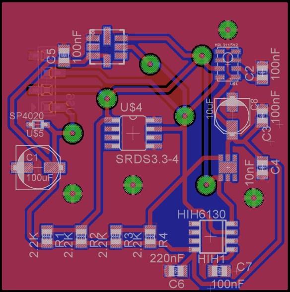
The board I will be making is a Temperature, Humidity, and Pressure sensor board for my updated weather station I’ve been working on. I will discuss the actual functioning of the board in a future post, but this post will focus on the manufacture of the double sided PCB itself. The first step in making the board, is designing it in Eagle, and if you are unfamiliar with Eagle, Sparkfun Tutorials are the best place to start to learn this free, fully functioned software. I like to use surface mount devices, because I can fit more in a limited space, but I do not push the limits as to size; I uses 0805 components whenever I can, because they are fairly small, but not so small I cannot manually place them on the board. I also make as many of the traces 24Mils as much as possible, and keep the traces separated as much as possible, just to make manufacture easy and forgiving. I use ground planes, with 16 Mill isolation, so I don’t have to etch off as much copper, so that part of the process is quicker. Finally, since I just solder a wire between the top and bottom for the vias, I create very large Via pads, 100 Mil in diameter, and make sure to use the thermal relief on the vias that connect the ground planes (there is a checkbox in the DRC settings, on the Supply tab, to do this), or the solder just flows all over the place on the ground plane.
I initially tried to use the toner transfer method, but the toner used in my Brother printer just doesn’t work for toner transfer. Even when I printed toner from and HP printer, though, the PCB I made just did not turn out as sharp as when I use photosensitive PCB and UV light. Single and double sided photoresist coated boards are available on eBay fairly inexpensively, just search for presensitized PCB. The brand name is I have used most often is Kinsten, but that is about all I can read because most of the package is in Chinese, but, never-the-less they seem to give good result to me. I would not recommend buying the photoresist you can paint on a copper clad board, because it is very difficult to get an even coat on the surface of the PCB, and the result suffer. The presensitized PCBs comes in about 4″ x 6″ size, so I normally must cut them before they are used ( I don’t usually make that large a PCB). In this case, the PCB is 1.75″ X 1.75″, and I just use a Dremel with a cutting wheel, to cut the PCB out. It turns out that it is really important to have good edges on the board because when you cut the board with the Dremel you will get a ridge around the cut line, which will prevent the negative from sitting flush on the photoresist during exposure, and cause blurry, unusable transfers. I make sure to bevel the cut edges.
Getting the images on both sides of the PCB to line up is probably the trickiest part of the whole operation. I solve this by drilling the holes in the board first, and use them a registration points. In order to do that, though, I needed a CNC drill. The Shapeoko project provides the perfect tool for this; inexpensive and very educational (what I learned from building this really helped when I built a 3 D printer). It is a full lightweight CNC router, and can be used to cut the PCB out of the 4X6 stock, if you need high accuracy or a weird shape. If you follow the excellent Spark Tutorials on using eagle to create a PCB, a drill file will be created in Excellon format. To convert this to gcode that Shapeoko will use, you can use a lot of free software, like Excellon To GCode Converter. Once you have the gcode, you can drill the holes in the PCB:
Once the holes are drilled, I print the pattern of the PCB’s top and bottom copper layer onto laser transparency “paper”. I use 3M Transparency Film CG5000, because I could get 50 sheets cheap on eBay , but any laser printer transparency will probably work. You can print this directly of of Eagle; just print the top layer (or bottom), pads, and via layers onto the transparency. The top layer must be printed as a mirror image because you want the printed side down, to touch the photoresist, so no blurring occurs because of light entering the side of the thickness of the transparency. You can align the transparency with the drilled holes for the Vias, and expose it to UV. I’m very frugal with my transparencies. Eagle lets you print the images on the top right, top center and top left, so I just keep sending the same transparency through the printer and print all the images I need on the same sheet. In this case, I need 4 transparencies, but I get all of them printed on one sheet, and still have space to spare for the next project.
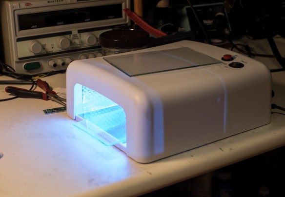
My UV exposure system is another eBay special. For about $17 dollars you can get a UV Fingernail Polish Dryer which works perfectly for small PCBs (I don’t know how safe it is to stick you hand in one of these, but using it to expose PCBs is pretty safe). The unit has 4 9Watt UV bulbs, 2 on top and 2 on the sides. I removed the 2 side bulbs, because I don’t what the light coming in from that angle and blurring the exposure. With just 2 bulbs in the device, the 120 second timer included on the device is just the right exposure time to get a good image. I put a piece of 4 x 6 glass on top of the aligned transparency/PCB to hold it flat, slide it into the chamber on the plastic base the unit comes with, press the 120 second timer, and when the UV lights turn off, that side of the PCB is exposed properly. I flip the PCB over and align the other transparency for the bottom copper, and expose it in the same way.
After the PCB is exposed, it is time for the chemistry experiments. The developer is for the presensitized board is called DP50, and is also available very cheaply on eBay. I have a dedicated tray that I use only for this process, and I mix 10 grams of developer into 200 grams of hot water. It only takes a minute to develop the board, and leaving it in too long will over develop the board and ruin the image. You can just look at the board, and when you have nice sharp edges on the traces, with no photoresist on the parts that are suppose to be clear of copper, run the board under water to stop the development process.
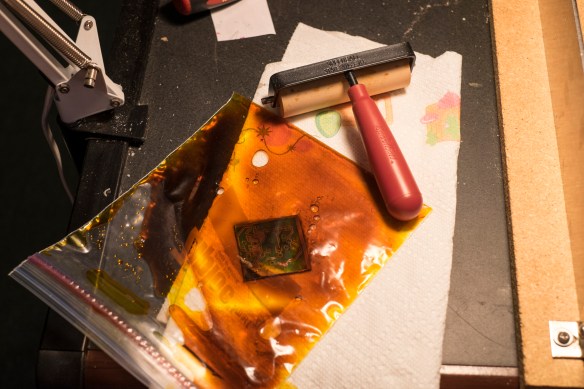
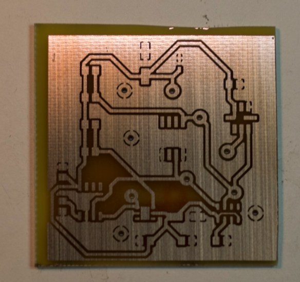
The messiest part of the process is etching; the process of removing the copper from the board to create the traces. I have tried using both Sodium Persulfate and Ferric Chloride. Sodium Persulfate has the advantage of being clear, so you can follow the etching process more easily, and know when you are done, but it is slower. Even though Ferric Chloride is about one of the most noxious chemical you are going to run across, it does do a better job of etching. I used to do the normal method of dumping the etchant and PCB into a tray and and shake it about to agitate it, and it was fairly slow; about an hour and a half to etch a board like this. I read this article, which gave a new approach to getting the etchant in touch with the copper, and it seems to improve the process (I don’t actually use any of the products this web site is pitching, though). I basically put a couple of ounces of Ferric Chloride in a heavy duty plastic bag, and use a squeegee to force the etchant over the surface of the PCB. In this case, it took about 12 minutes to etch this PCB. I do all of this very carefully, to prevent rupturing the bag, and I wear latex gloves, and do it on a bed of paper towels, just to try to contain the liquid, but I also wear old clothes because someday it will make a mess.
At this point I have a PCB that would be acceptable as a break out board, or something that would be used in the lab, but it is not something I would use as an end product for a project I was working on. Part 2 will document the procedure of adding a solder mask, tinning the contacts, and reflow solding the components.


