About kevinmkessler

Blogs about my Electronic projects

Transformerless Power Supply Characterization

I’m working on a project that uses Bluetooth LE to control power outlets.  One day, an Amazon special popped up for a set of Etekcity ZAP power control device, and at $20 for 5 power outlet controllers and 2 remotes, I decided to buy just to look at how they worked.  The idea is you configure the remote to switch on and off each outlet controller, and I guess you walk around your house with the remote to turn your light on and off.  While I don’t really know why you would want to do that, it turned out I really like the form factor of the controller.

ZapOpening it up, I found some microcontroller that they scraped off the markings, and a 433MHz receiver, just like the ones you can buy from eBay or AliExpress.  It also had a 10 Amp relay that did the actual switching, protected by a thermal fuse.  It was powered by a transformerless power supply, something I knew little about, except always hearing that they were dangerous and bad.

I decided I could retrofit these units with my Bluetooth module, so I removed the 433MHz receiver, microcontroller, and 5V linear regulator because my project needed 3.3V. I knew from my research on the transformerless AC power supplies that they could not provide much current, so I decided to do some testing to see if it was adequate for my needs.

Hooking up my trusty Maynuo M9711 Electronic Load, I ran the power supply of the device through various current loads, and got the following graph:

TransformerlessPS

Basically the voltage hangs up around 25 Volts up to about 25mA load, and then it drops off a cliff.  Interestingly, once you get past the knee area, backing the current off a little does not cause the power supply to recover.  You have to pull the current way back to 15mA or so before the voltage recovers back to its 25V, which means the power supply is not very forgiving of over current situations.  Since my BLE module uses about 15mA, and the power supply must also supply current for the relay when it is powered on, just slapping a 3.3 V linear regulator after this power supply would not give a very large margin for error.

On AliExpress you can find these nifty MP1584 based buck converters that are less than an inch square, and cost less than 50 cents.  They come with a really crappy surface mount potentiometer, which really can’t keep a stable setting, so the voltage bounces around a lot.  I pulled that pot off and soldered an 0805 24K resistor in its place that fits perfectly in the footprint of the pot, and gives me 3.15 Volts solid.  That voltage is right in the middle of the range for the NRF51822 based BLE modules, so that works well.

BuckModule

I tested the load characteristics of the buck converter powered by the transformerless AC power supply, monitoring both the buck converter’s current and voltage, and the transformerless power supply’s current and voltage.

TestSetup

The results are very promising:

BuckChart

The buck converter’s voltage stay constant until the current reaches about 125mA, after which everything falls apart. A current budget of 120mA or so, though, is much more than I will need for my project.

Monitoring both the input voltage and current and output voltage and current of the buck converter allows me to calculate the efficiency of the convert by dividing the output power by the input power.  Under these conditions this buck convert was only about 68% efficient, not very good for a dc switching regulator, but good enough for this use case.


How I Make a PCB Part 2

To give the board a professional look, and to help prevent solder bridges, I like adding a solder mask.  I use a photosensitive dry film mask I bought on eBay, which gets laminated to the PCB, exposed to UV, and developed.  This Instructable gives very detailed instructions on the entire procedure.

Laminator with PCB ready for development

Laminator with PCB ready for development

After the solder mask is developed, I occasionally tin the board.  Tinning the board should help protect the copper, and it looks nice, but the tinning solution is expensive, so I don’t do it often.  Since this board will be installed outside, though, I decided to give it the full treatment and tin the PCB.  I use MG Chemicals 421 Liquid Tin, and it is very easy to use; just pour the liquid into a plastic container with the PCB, and in about 5 minutes, all the exposed copper will have a tin coating.

PCB soaking in the Liquid Tin solution

PCB soaking in the Liquid Tin solution

At this point I’m ready to reflow the components.  The hardest part of the whole process is to apply the solder paste.  Since I don’t make a solder stencil, I have to apply the paste by hand.  I squirt some solder paste onto a card, and thin the paste with some flux so that the paste is only about half as viscous as it was originally.  Then I take a toothpick, and gently dab the pads with the thinned paste, making sure I do not put too much paste on the pad; this is one of those cases where less is more.  Now it is time to place the components, and I use some good magnifier glasses and an eBay QS-2008 Vacuum Pen, which, for less than $25, works surprisingly well. The PCB and the placed components are then put into my slightly modified Black And Decker Convection Toaster Oven.  The only modification I made to was to drill a hole though the interior, and glue a thermocouple in place with QuikSteel high temperature glue.  I would love to be able to create an oven controller to have the oven generate the proper temperature profile for the solder paste, but the oven itself cannot heat up quickly enough to match the profile.  Right now, I just plugin my multimeter to the thermocouple, crank the oven to maximum, and wait until the temperature hits 215-220 degrees C and turn off the oven. I do wrap the oven in a welder’s blanket to try to increase the insulation, but I think I need to add a couple extra heating elements into the oven, if I want to generate a correct temperature profile.

Reflow Oven with Multimeter Temperature Gauge

Reflow Oven with Multimeter Temperature Gauge

The only thing left to complete this PCB is to verify the reflowed solder joints.  In this case, the TVS diode had tombstoned a bit and had to be hand soldered.  Then hand solder the vias and connector, and the PCB is complete.

Completed PCB

Completed PCB


How I make a PCB Part 1

Over the years, I’ve tried many different techniques for creating PCBs, and this blog will document the way that works best for me now.  This post will document the basic procedure I use to create a PCB to something that is usable.   Part 2 will show how I make a “deluxe” PCB, for an application such as this one which will have to survive the elements outdoors.

The board I will be making is a Temperature, Humidity, and Pressure sensor board for my updated weather station I’ve been working on.  I will discuss the actual functioning of the board in a future post, but this post will focus on the manufacture of the double sided PCB itself.  The first step in making the board, is designing it in Eagle, and if you are unfamiliar with Eagle, Sparkfun Tutorials are the best place to start to learn this free, fully functioned software.  I like to use surface mount devices, because I can fit more in a limited space, but I do not push the limits as to size;  I uses 0805 components whenever I can, because they are fairly small, but not so small I cannot manually place them on the board.  I also make as many of the traces 24Mils as much as possible, and keep the traces separated as much as possible, just to make manufacture easy and forgiving.  I use ground planes, with 16 Mill isolation, so I don’t have to etch off as much copper, so that part of the process is quicker.  Finally, since I just solder a wire between the top and bottom for the vias, I create very large Via pads, 100 Mil in diameter, and make sure to use the thermal relief on the vias that connect the ground planes (there is a checkbox in the DRC settings, on the Supply tab, to do this), or the solder just flows all over the place on the ground plane.

SparkSensorPCB

Double Sided Sensor Board PCB

I initially tried to use the toner transfer method, but the toner used in my Brother printer just doesn’t work for toner transfer.  Even when I printed toner from and HP printer, though, the PCB I made just did not turn out as sharp as when I use photosensitive PCB and UV light.  Single and double sided photoresist coated boards are available on eBay fairly inexpensively, just search for presensitized PCB.  The brand name is I have used most often is Kinsten, but that is about all I can read because most of the package is in Chinese, but, never-the-less they seem to give good result to me.  I would not recommend buying the photoresist you can paint on a copper clad board, because it is very difficult to get an even coat on the surface of the PCB, and the result suffer.  The presensitized PCBs comes in about 4″ x 6″ size, so I normally must cut them before they are used ( I don’t usually make that large a PCB).  In this case, the PCB is 1.75″ X 1.75″, and I just use a Dremel with a cutting wheel, to cut the PCB out.  It turns out that it is really important to have good edges on the board because when you cut the board with the Dremel you will get a ridge around the cut line, which will prevent the negative from sitting flush on the photoresist during exposure, and cause blurry, unusable transfers.  I make sure to bevel the cut edges.

Getting the images on both sides of the PCB to line up is probably the trickiest part of the whole operation.  I solve this by drilling the holes in the board first, and use them a registration points.  In order to do that, though, I needed a CNC drill.  The Shapeoko project provides the perfect tool for this; inexpensive and very educational (what I learned from building this really helped when I built a 3 D printer).  It is a full lightweight CNC router, and can be used to cut the PCB out of the 4X6 stock, if you need high accuracy or a weird shape.  If you follow the excellent Spark Tutorials on using eagle to create a PCB, a drill file will be created in Excellon format.  To convert this to gcode that Shapeoko will use, you can use a lot of free software, like Excellon To GCode Converter.  Once you have the gcode, you can drill the holes in the PCB:

ShapeOkoDrilling

Shapeoko Drilling holes in the PCB

Once the holes are drilled, I print the pattern of the PCB’s top and bottom copper layer onto laser transparency “paper”.   I use 3M Transparency Film CG5000, because I could get 50 sheets cheap on eBay , but any laser printer transparency will probably work.   You can print this directly of of Eagle; just print the top layer (or bottom), pads, and via layers onto the transparency.  The top layer must be printed as a mirror image because you want the printed side down, to touch the photoresist, so no blurring occurs because of light entering the side of the thickness of the transparency.  You can align the transparency with the drilled holes for the Vias, and expose it to UV.  I’m very frugal with my transparencies.  Eagle lets you print the images on the top right, top center and top left, so I just keep sending the same transparency through the printer and print all the images I need on the same sheet.  In this case, I need 4 transparencies, but I get all of them printed on one sheet, and still have space to spare for the next project.

My UV exposure system is another eBay special.  For about $17 dollars you can get a UV Fingernail Polish Dryer which works perfectly for small PCBs (I don’t know how safe it is to stick you hand in one of these, but using it to expose PCBs is pretty safe).  The unit has 4 9Watt UV bulbs, 2 on top and 2 on the sides.  I removed the 2 side bulbs, because I don’t what the light coming in from that angle and blurring the exposure.  With just 2 bulbs in the device, the 120 second timer included on the device is just the right exposure time to get a good image.  I put a piece of 4 x 6 glass on top of the aligned transparency/PCB to hold it flat, slide it into the chamber on the plastic base the unit comes with, press the 120 second timer, and when the UV lights turn off, that side of the PCB is exposed properly.  I flip the PCB over and align the other transparency for the bottom copper, and expose it in the same way.

Alignment

Aligning the transparency to the PCB with the drilled holes

Exposure

Exposing the photoresist with UV light

After the PCB is exposed, it is time for the chemistry experiments.  The developer is for the presensitized board is called DP50, and is also available very cheaply on eBay.  I have a dedicated tray that I use only for this process, and I mix 10 grams of developer into 200 grams of hot water.  It only takes a minute to develop the board, and leaving it in too long will over develop the board and ruin the image.  You can just look at the board, and when you have nice sharp edges on the traces, with no photoresist on the parts that are suppose to be clear of copper, run the board under water to stop the development process.

The messiest part of the process is etching; the process of removing the copper from the board to create the traces.  I have tried using both Sodium Persulfate and Ferric Chloride.  Sodium Persulfate has the advantage of being clear, so you can follow the etching process more easily, and know when you are done, but it is slower.  Even though Ferric Chloride is about one of the most noxious chemical you are going to run across, it does do a better job of etching.  I used to do the normal method of dumping the etchant and PCB into a tray and and shake it about to agitate it, and it was fairly slow; about an hour and a half to etch a board like this. I read this article, which gave a new approach to getting the etchant in touch with the copper, and it seems to improve the process (I don’t actually use any of the products this web site is pitching, though).  I basically put a couple of ounces of Ferric Chloride in a heavy duty plastic bag, and use a squeegee to force the etchant over the surface of the PCB.  In this case, it took about 12 minutes to etch this PCB.  I do all of this very carefully, to prevent rupturing the bag, and I wear latex gloves, and do it on a bed of paper towels, just to try to contain the liquid, but I also wear old clothes because someday it will make a mess.

Etching

Ferric Chloride in a plastic bag to force the etchant to more quickly remove the copper.

At this point I have a PCB that would be acceptable as a break out board, or something that would be used in the lab, but it is not something I would use as an end product for a project I was working on.  Part 2 will document the procedure of adding a solder mask, tinning the contacts, and reflow solding the components.

EtchedPCB

PCB After Etching

2 Line LCD Display

Since moving away from using an Arduino for projects and using microcontrollers directly, I’ve lost the nice facility the Arduino has for sending debug information out the USART to the PC for display.  It’s also very easy to connect to the Arduino to the PC for programming, since it is simply a USB connection.

I decided to build a little circuit board which contained a 16 character by 2 line display based on the HD44780 chipset.  This is normally a parallel device taking at least 6 pins to operate (10 in 8 bit mode), but my first project I was going to use the 16×2 LCD display was based on a ATTiny85 processor (8 pins total on the device), so I had to roll my own serial interface for the device.  I decided to use an SPI interface, which had the added benefit that once I connected my debugging display to the SPI interface, I already had connections to the pins used by the TinyUSB programmer, so I was able to kill 2 birds with on stone; interface a debugging display and a programmer with a minimal set of breadboard wires.

LCD Breadboard Debugging Tool

LCD Breadboard Debugging Tool

The circuit is very simple, with a 74LS595 Shift Register converting the serial data transmitted through the MOSI pin of the AVR chip, clocked by the SCK pin, and latched to the output through the SS pin.

LCD Debugger Schematic

LCD Debugger Schematic

The board also includes pots for contrast and brightness of the LCD display, a reset switch, and the connector for the programmer.

The software to drive the display borrows heavily from this blog which describes interfacing this display to a PIC microcontroller.  The code is fairly straightforward; you need to define the pins for the MOSI, SCK, and shift register latch, and then you can start LCDSendString’s to the display.  Since the ATTiny85 does not have API, a bit-banged version of the code is included within the proper #if defined blocks.  The code is located on GitHub here: https://github.com/kevinkessler/LCD2Line

Sample code to use the display would look like:

#include "LCD2Line.h"

int main (void)
{
    LCDinitSPI();
    LCDInit();
    LCDSetDisplay(1,0,0);  // Turn on display, Turn off cursor
    LCDSetDDramAddr(0x00); // Sets display to 1st character on the 
                           // first line
    LCDSendString("Hello");
    LCDSetDDramAddr(0x40); // Set display to 1st character on the 
                           // second line
    LCDSendString("World");

    while(1){};
}

dasKeyboard Repair

There are some of us out there who really can’t stand typing on the cheapo $5 keyboards that come with computers these days and will spend $130 on a very clicky keyboard.  I’m old school, and I started my career using IBM PS/2s with the very heavy and very precise keyboards, and, in fact, I used one of the original PS/2 keyboards for 20 years until it gave up the ghost.  Now, I always use one of the many modern clones of these keyboards on all my computers.  At work, I use a dasKeyboard Model S, but the forward slash/pipe key broke, which is a pretty important key for people who spend a good bit of time working at DOS and Linux shells.

Much like the human body, where they can take some “extra” tendons you have laying around in your body, and fix your ACL, there are plenty of “extra” keys on the dasKeyboard I could use to replace my broken key.  In this case, I used the right Windows key, which I doubt I have ever used (I use ALT-ESC if I want to bring up the start menu with a keystroke).  When you pull the keycap off of the key, you find the switch mechanism:

KeySwitch and I was able to unsolder the broken switch and replace it with the one under the windows key.

This picture shoes the location of the screws.  You have to pull off 2 of the rubber feet to get to screws, and it is important to note that there is no screw under the label, even though it feels like there is one (you can see I ripped up the label trying to find it).

screws

Once you open up the case, which takes a bit of force, you will need to unscrew the PCB, because the ribbon cable does not come off.

PCB

At this point the hard part is over.  Using some resin and desolder braid, it is pretty easy to unsolder the keys from the main PCB of the keyboard.  Getting the keys off the PCB takes a bit of work, because there are some clips on the font side that you just have to pry a little, and pushing the center pin on the back side will eventually pop the key right off the board.  The arrows show where the keys were originally:

DesolderedKeys

You can then just solder the new key in place.

The finished product.  I’ve opened a case with dasKeyboard to find out if I can buy a new key, but if not, or it is too expensive, I will probably solder the broken key into the hole just to cover the spot.

Whole

Update: The key switches are a standard part, Cherry MX MX1A-E1NW, for the blue capped models.  You can get them at Mouser, Digikey, Newark14, and other places.

Telemetry Bridge

Bridging the Telemetry from and APM Quadcopter Controller to a Spektrum Telemetry Module

I came across this post on the RCGroups forum describing how to interface into the Spektrum Telemetry Module and send your own telemetry to a Spektrum radio.   I was building my own Quadcopter centered around the APM flight controller, which is based on an Arduino  Mega 2560.  One of the options on this controller is to put a radio transmitter on the Serial 1 port, and a radio receiver on a PC, and the controller can continuously transmit telemetry information like GPS coordinates, Battery Current and Voltage, Altitude, etc., to software running on the PC.  Since the Spektrum Telemetry is and I2C master, and the APM is sending the telemetry out a serial USART, I thought it would be a fairly straight forward task to use an ATMega 328p to read the telemetry stream from the APM, reformat it and send it on to the Spektrum Telemetry module.

While I will also have a fondness for the Arduino, because it got me started work with microcontrollers, I’ve moved away from using the Arduino in my projects because even a small Arduino is big (compared to the atmega chip itself), expensive and the software is somewhat limited.  In this case, the AVR had to respond to several I2C slave addresses (but not others), and the Arduino Wire interface is not well suited for that, but coding directly to the I2C interface made this possible.

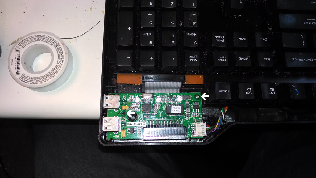
The circuit board I made for this project consists of an ATMega 328p running at 16MHz and 5 V (because you need to run at 5 Volts to be in spec for 16MHz), a voltage level shifter to interface the 5 V I2C interface on the AVR to the 3.3 V Spektrum telemetry module, and connectors for the ISP interface, and a Bluetooth module I use to configure the Quadcopter with my phone.  I used parts I had in my inventory, so some of the components, like the 1 Amp 3.3 V regulator and the 1 Amp diodes are not what I would us if I was ordering parts just for this project.

sch

The circuit board is also designed for my home made PCB process (very large VIA pads), and would not be ideal for a professional PCB fabricator.

brd

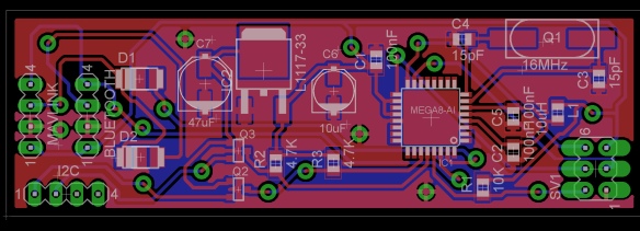
The raw Eagle files are located on my GitHub site along with the source code.

Board

The serial stream that comes out of the APM is a protocol called Mavlink, and I spent a good bit of time on their site trying to figure out how to make this work.  First, you have to download the Mavlink include files here, and generate them with a Python script.  After running into some problems, I found that the structure  __mavlink_request_data_stream_t in common/mavlink_msg_request_stream.h was incorrect (the order of the fields was wrong).  It should look like:


typedef struct __mavlink_request_data_stream_t
{
uint8_t target_system; ///< The target requested to send the message stream.
uint8_t target_component; ///< The target requested to send the message stream.
uint8_t req_stream_id; ///< The ID of the requested data stream
uint16_t req_message_rate; ///< The requested interval between two messages of this type
uint8_t start_stop; ///< 1 to start sending, 0 to stop sending.
} mavlink_request_data_stream_t;

The other important Mavlink setting it know about when using a uC is at the top of main.c, before the include of mavlink.h:


// Save memory, MAVLINK by default allocates 4 256 byte buffers
#define MAVLINK_COMM_NUM_BUFFERS 1


#include <stdio.h>
#include <stdlib.h>

If you don’t set the number of buffers to 1 before you include mavlink.h, you will waste 768 bytes of SRAM, which the AVR does not have to spare.

A most invaluable tool for debugging both the Serial connections and the I2C I’ve found is a logic analyzer.  I use the Saleae Analyzer, which I am very happy with.  It would have been very difficult to do this without being able to see exactly what was going on the wires.

Quad hooked up to a logic analyzer

Quad hooked up to a logic analyzer

On the Telemetry side of the process, when the unit is powered on, the Telemetry module requests data from the I2C slaves from address 0x00 to 0x7D twice (0,0,1,1,2,2,etc.).  The bridge has to respond to the slave addresses it is going to fulfill (the RCGroups post above provide the list of slave addresses and functions) during this initialization, or that slave address will not be polled.  The AVR cannot answer to addresses 0x00 and 0x01, because they are for internal use of some sort.  The module Spektrum.c has a list of addresses the AVR will respond to, and, since during initialization the addresses are polled in numeric order, it sets the slave address of the AVR to the lowest address, and once that slave address has been called twice, the code resets the slave address to the next value, and so on util it has hit every address in the list.  The AVR responds to the telemetry unit with the 16 byte response packet with 0 values.

uint8_t addresses[]={0x03,0x0A,0x11,0x12,0x16,0x17,0x00};

ISR(TWI_vect)
{
    switch (TW_STATUS)
    {

        case TW_ST_SLA_ACK:
        if(initializing)
        {
            addrCount++;
            if(addrCount==2)
            {
                addrCount=0;
                if(addresses[++addrIdx]==0)
                {
                    TWAR=addresses[0]<<1;
                    initializing=0;
                }
                else
                    TWAR=addresses[addrIdx]<<1;
            }
    }
    else
        TWAMR=0xFF;

After the initialization phase, the telemetry unit will only poll the slaves that responded during initialization, so the address mask, TWMAR, is set to 0xFF, which means the AVR will respond to any slave address.  When any request for data is sent to the AVR after initialization, it looks at the address that is being requested, and sends the correct buffer back to the master.  Another important thing to note is the telemetry unit does not poll the slave addresses until the radio it is bound to is up and ready to receive data, so if the radio is off, the initialization will occur, but no polling of the slave will occur until the raid is turned on.

One final thing to note is that the AVR does not have division natively built into the instruction set, so it is an expensive operation. Since the AVR needs to be available to handled the asynchronous requests from 2 outside feeds, it has to get the calculations done as quickly as possible .  To get around this, a technique called fixed point arithmetic can be used.  This article has an excellent description of the technique.  For example, the following is a division by 10,000,000.

uint16_t divideBy1E7(uint32_t dividend)
{
	return (uint16_t)((((int64_t)dividend * 0xD6E0LU) >> 16) >> 23);
	//return (uint16_t)(dividend / 1E7);
}

In the source code there is a #define constant called TIMEIT which will include code to time the number of clock cycles the AVR takes to compute the GPS buffers (the most mathematically complex part of the code), and display that value in the Power Box 2nd battery capacity (which is normally 0).  I tested the code with the straight-forward division and with fixed point, and compiled with full optimizations (-o3), the fixed point version of the setGPSBuf call took about 46,500 clock cycles while the division averaged 56,500 clock cycles.  I’m not sure a 17.5% improvement was worth the effort of figuring out the fixed-point parameters, but it was interesting.

As I said above, all the code and eagle files are located on GitHub.
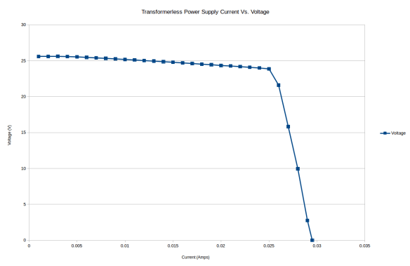
Sparkfun Weather Station

I installed the Sparkfun Weather Meters mainly for the rain gauge.  It is quite expensive, and didn’t even come with the small screws which hold the anemometer and wind vane to the support arm.  It does seem to be well made, and makes my system look like a weather station.

Sparkfun Weather Meters in the wild

The datasheet shows that the rain gauge and the anemometer are magnetic reed switches; every 0.011″ of rain causes a momentary contact and a 2.4km/h wind will cause a momentary contact every second for the anemometer.  These inputs will be connected to Arduino interrupts.  The wind vane uses an array of resistors which can be read through the ADC of the Arduino, but the datasheet is wrong for the wind vane.  At 315°, the datasheet states that the voltage should be 4.78V, but in actuality, with a 10K resistor in series with a 64.9K resistor, the voltage drop across the vane will be 4.33V.

The following code setups up the inputs and the interrupts to read this device.  Note that setting a pin to INPUT and then writing a HIGH value to it turns on the internal 20K pull up resistor in the Arduino, which prevents the need for external pull up resistors on the interrupt driven devices.  The wind vane requires a 10K resistor in series with the vane’s resistors, and to save power, this resistor and the vane are powered from a digital output, which is driven HIGH only when the reading is to be taken.

#define ANEMOMETER_PIN 3
#define ANEMOMETER_INT 1
#define VANE_PWR 4
#define VANE_PIN A0
#define RAIN_GAUGE_PIN 2
#define RAIN_GAUGE_INT 0

void setupWeatherInts()
{
  pinMode(ANEMOMETER_PIN,INPUT);
  digitalWrite(ANEMOMETER_PIN,HIGH);  // Turn on the internal Pull Up Resistor
  pinMode(RAIN_GAUGE_PIN,INPUT);
  digitalWrite(RAIN_GAUGE_PIN,HIGH);  // Turn on the internal Pull Up Resistor
  pinMode(VANE_PWR,OUTPUT);
  digitalWrite(VANE_PWR,LOW);
  attachInterrupt(ANEMOMETER_INT,anemometerClick,FALLING);
  attachInterrupt(RAIN_GAUGE_INT,rainGageClick,FALLING);
  interrupts();
}

In order for the anemometer to be accurate, any surrounding objects must be 4 time as far as they are higher than the anemometer.  For example, if my anemometer is 5 feet off the ground, and my house is 25 feet tall, the anemometer would need to be 80 feet from the house to be able to measure the wind speed accurately.  In my case, nothing close to this leeway is possible, but I still setup the anemometer just for the educational experience.

Every rotation of the anemometer causes a call to the interrupt service routine anemometerClick().  Switch debouncing is accomplished by assuming any interrupt that occurs within 500 uS of the previous one is a bounce and should be ignored.  This limits the max speed this configuration can measure to about 2900 miles per hour, but since I don’t live on Jupiter I think I can live with this compromise.  The getUnitWind() function returns the average wind speed since the last poll, which is every 60 seconds.  The getGust function uses the shortest time between 2 interrupts to calculate the fastest wind speed since the last poll.

#define WIND_FACTOR 2.4
#define TEST_PAUSE 60000

volatile unsigned long anem_count=0;
volatile unsigned long anem_last=0;
volatile unsigned long anem_min=0xffffffff;

double getUnitWind()
{
  unsigned long reading=anem_count;
  anem_count=0;
  return (WIND_FACTOR*reading)/(TEST_PAUSE/1000);
}

double getGust()
{

  unsigned long reading=anem_min;
  anem_min=0xffffffff;
  double time=reading/1000000.0;

  return (1/(reading/1000000.0))*WIND_FACTOR;
}

void anemometerClick()
{
  long thisTime=micros()-anem_last;
  anem_last=micros();
  if(thisTime>500)
  {
    anem_count++;
    if(thisTime<anem_min)
    {
      anem_min=thisTime;
    }

  }
}

When the system included the logger shield, SRAM memory was so tight that I had to move variable data from SRAM to FLASH.  Using PROGMEM allowed me to move the vane directions and the expected values out of SRAM, and in itself saved almost 100 bytes of the 2000 the Arduino has (moving String values in addition freed up about 500 bytes of SRAM).  The pgm_read_word function pulls the values out of FLASH and into SRAM when needed, but only works with integers, so the actual wind directions are stored as 10X their value.

As mentioned in the MCP9700 post, the analogReference for the Wind Vane must be switched from the 1.1V the MCP9700 was using to the 5V default value.  Since it takes some time for the ADC to adjust to the new reference, the first 10 adc readings are just thrown out.

To save battery power, the wind vane is powered by the digital pin VANE_PWR right before it is used.  a 100ms delay is inserted after the power pin is driven high just to left things settle down.  The rest of the function compares the ADC value to the ideal values in vaneValues, and returns the corresponding wind direction.


static int vaneValues[] PROGMEM={66,84,92,127,184,244,287,406,461,600,631,702,786,827,889,946};
static int vaneDirections[] PROGMEM={1125,675,900,1575,1350,2025,1800,225,450,2475,2250,3375,0,2925,3150,2700};

double getWindVane()
{
  analogReference(DEFAULT);
  digitalWrite(VANE_PWR,HIGH);
  delay(100);
  for(int n=0;n<10;n++)
  {
    analogRead(VANE_PIN);
  }

  unsigned int reading=analogRead(VANE_PIN);
  digitalWrite(VANE_PWR,LOW);
  unsigned int lastDiff=2048;

  for (int n=0;n<16;n++)
  {
    int diff=reading-pgm_read_word(&vaneValues[n]);
    diff=abs(diff);
    if(diff==0)
       return pgm_read_word(&vaneDirections[n])/10.0;

    if(diff>lastDiff)
    {
      return pgm_read_word(&vaneDirections[n-1])/10.0;
    }

    lastDiff=diff;
 }

  return pgm_read_word(&vaneDirections[15])/10.0;

}

The rain gauge work much like the anemometer in that it drives an interrupt, and a 500us debounce time is used.  The interrupt the simply counts the number of switch contacts that occurred since the last poll and multiplies that by the number of mm of rain each switch contact represents.

#define RAIN_FACTOR 0.2794

volatile unsigned long rain_count=0;
volatile unsigned long rain_last=0;

double getUnitRain()
{

  unsigned long reading=rain_count;
  rain_count=0;
  double unit_rain=reading*RAIN_FACTOR;

  return unit_rain;
}

void rainGageClick()
{
    long thisTime=micros()-rain_last;
    rain_last=micros();
    if(thisTime>500)
    {
      rain_count++;
    }
}

MCP9700

Soil temperature is one of the things the Garduino monitors.  Unfortunately, soil is a harsh environment and replacing a $1.50 TMP36 everything time one stopped working was becoming a bit of a drag, so I looked for something cheaper.  The MCP9700 is a temperature sensor available from Mouser.com for $0.34, and at that price, I feel a little more free to experiment with waterproofing these sensors.

These devices are pretty nice to work with, since they can take a supply voltage of 2.1 to 5.5V and the output pin will be at .5V at 0° C and rise 0.01V for every rise in 1°C.  This document  describes how to compensate for 2nd order effects to increase accuracy further.

It is critical to put a capacitor between the Vout pin in ground (about 2nF), because without it, there is a 27kHz wave that appears on the output.  In my tests, Vout oscillated 0.0575 Volt P-P, which represents a variation of 5.75 °C from reading to reading.  With the capacitor between Vout and GND, the variation between readings drops to about 0.5°C.

The code for reading the temperature of these devices is pretty straightforward:

float readMCP9700(int pin,float offset)
{
  analogReference(INTERNAL);
  for (int n=0;n<5;n++)
    analogRead(pin);

  int adc=analogRead(pin);
  float tSensor=((adc*(1.1/1024.0))-0.5+offset)*100;
  float error=244e-6*(125-tSensor)*(tSensor - -40.0) + 2E-12*(tSensor - -40.0)-2.0;
  float temp=tSensor-error;

  return temp;
}

In my application, I have some ADC calls done against the 5V analogReference, and the analogReads for the MCP9700 are done against the internal 1.1V reference.  According to the ATMega328 datasheet, when switching between references, you should throw out the reading immediately after the switch, because it will be inaccurate.  In this function, I throw out  5 readings after setting the analogReference, just to give it extra time to settle down, and then I take the real measurement.  The 2nd order error is calculated as described in the accuracy compensation document mentioned above.

I also pass in an offset to allow me to adjust each individual sensor against a know temperature.  In my case, I really didn’t have a know temperature reading I thought was any more accurate than anything else I had, so I setup 4 MCP9700s and let them read the same temperature.  I averaged these readings, and I pass in the offset for each individual MCP9700 from that average, so, if nothing else, the temperatures read between these 4 devices will be consistent.  The offsets were on the order of 0.01V.

MAX44009

One of the questions I wanted to answer with my Garduino was how much light is lost through the plastic covering of the Greenhouse.  What I have found is it is very difficult to find a light sensor that has the dynamic range from darkness to full sun, but I finally stumbled on the MAX44009, which has a range from 0.045 to 180,000 Lux.  The downside of this device is no one is making a breakout board for it, so I was on my own.

Homemade breakout board for the MAX44009

Yes, this beautiful homemade PCB does work.  I made it by the laser toner transfer method, but my home printer, a Brother HL-4040CN did not work; the toner did not stick to the copper board no matter how long I put the iron on it.  I ended up creating a PDF file with Gerber2PDF and printing the image on some HP printers at work.  Unfortunately,  in my rush to not be caught screwing around with something that wasn’t work related, I forgot to make a mirror image of the PCB, so everything is backwards on the PCB.  Even with the HP toner, the toner transfer was not very good, but, considering the fact that the MAX44009 chip is 2mm x 2mm and the pads for the 6 pins are 0.36mm x 0.48 mm, the toner transfer was accurate enough to work.  Adding to the fact that this was the first time I used my hot air re-work station to do something constructive, you could have knocked me off my chair with a feather when the final assembly actually returned valid data.

It wasn’t a complete Eureka moment, though, because while the data sheet says the I2C address can be selected (with the AD pin) to be 148 or 150, that does not seem to be true.  I found this important utility, I2CScanner which runs through every I2C address, and shows which addresses a device is responding to.  This really saved me, because it showed that the real address of the MAX44009 was 203 (I forgot to note the address when AD is low, so I’ll document that when I make the improved version of the PCB).  Once I had the right address, interfacing with the MAX44009 is very straightforward, since it uses the I2C Wire Arduino  library:

#define MAX_ADDR 203

float getLux()
{
int luxHigh=readI2CAddr(0x03);
int luxLow=readI2CAddr(0x04);
int exponent=(luxHigh&0xf0)>>4;
int mant=(luxHigh&0x0f)<<4|luxLow;
return (float)(pow(2,exponent)*mant)*0.045;

}

int readI2CAddr(int addr)
{

Wire.beginTransmission(MAX_ADDR);
Wire.write(addr);
Wire.endTransmission();

Wire.requestFrom(MAX_ADDR,1);

int n=0;
for(n=0;n<25;n++)
{
if(Wire.available())
break;

delay(100);
}

if (n==25)
return 0;
else
return Wire.read();
}

I was expecting to have to handled the situation where I would have to programatically change the sensitivity of the device so that I would have to set longer integration times in low light conditions, and shorter ones in bright conditions, but the device handles that all by itself.  The device can be configured in a manual mode so that the user has control of exactly what integration time will be used for each reading, but in my case, the automatic setting behaved the way I wished.

I’ve created an Eagle library that contains the land pattern for the MAX44009.

I really like the I2C bus, but its major disadvantage is the max length which is reportedly pretty short.  I currently have the MAX44009 sitting off of about 2.5 M of 6 conductor satin cable, connected to the same 3.3V bi-directional voltage translator circuit my BMP085 is connected to, and it is working well.  I expect when I have to connect another MAX44009 to measure the light loss from inside the Greenhouse, though, the length will become a problem.  I will be researching some I2C bus lengthing techniques and will report on them in the future.

The waterproof enclosure for the MAX44009 consists of a plastic food container with a clear plastic cover, and the bottom cut out for ventilation.


This is the PDF for the Break Out Board that I used for the Toner Transfer method to create the PCB.

BMP085

The BMP085 is a I2C Barometric Pressure/Temperature sensor available from both Sparkfun and eBay.  The Sparkfun breakout board is very expensive, about $20, but they have excellent instructions on how to use it.  You can get the BMP085 chip on eBay for about $4 and the breakout board for about $6 for 3, but you have to be able to solder SMD to use them.

BMP085 breakout board soldered into my weather station interface board

Sparkfun has an excellent tutorial whose code I pretty much just used verbatim in my application. The only thing I changed were the bmp085Read and bmp085ReadInt functions, since as written, they will retry forever for the bmp085 to respond.  Since my device is outside, and attached to an I2C bus that is about 2.5 M long (for the Max44009 light sensor), sometimes I get a failure in reading the responses from the BMP085.  I just changed the lines that read


  while(!Wire.available())
    ;

To read:


  int n=0;
  for(n=0;n<25;n++)
  {
    if(Wire.available())
      break;

    delay(100);
  }

  if (n==25)
  {
    return 0;
  }

This way if my BMP085 malfunctions, the whole system doesn’t hang.  The other code adjustment was to put in the altitude compensation in the calculations:

#define ALT 142.0

float getPressure()
{
  long pa=bmp085GetPressure(bmp085ReadUP());

  float press=((float)pa/pow((1-ALT/44330),5.255))/100.0;
  return press;
}

Before I put in the compensation for altitude, my pressure was always too low.  Once I compensated for my 142 M altitude, the results from this device are spot on.  I’m very happy with the accuracy of this chip.

The other trick to using this device is the fact that it is a 3.3V device, and you can’t simply connect it up to a 5V I2C Arduino connection and hope for it to have a long life.  This document gives a very detailed discussion on setting up a bi-directional voltage level translator for the I2C bus.  The highlighted part of the schematic below shows the voltage level translator (the transistors are a couple of SN7000 MOSFETs):

Bi-Directional voltage translator for the I2C bus.